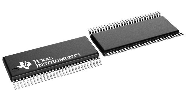
SN74ALVCF162835 Series
3.3-V CMOS 18-Bit Universal Bus Driver with 3-State Outputs
Manufacturer: Texas Instruments
Catalog
3.3-V CMOS 18-Bit Universal Bus Driver with 3-State Outputs
Key Features
• Member of the Texas Instruments Widebus™ FamilyIdeal for Use in PC133 Register DIMMTypical Output Skew . . . <250 psVCC= 3.3 V ± 0.3 V . . . Normal RangeVCC= 2.7 V to 3.6 V . . . Extended RangeVCC= 2.5 V ± 0.2 VRail-to-Rail Output Swing for Increased Noise MarginBalanced Output Drivers . . . ±18 mALow Switching NoiseLatch-Up Performance Exceeds 100 mA Per JESD 78, Class IIESD Protection Exceeds JESD 222000-V Human-Body Model (A114-A)200-V Machine Model (A115-A)1000-V Charged-Device Model (C101)Widebus is a trademark of Texas Instruments.Member of the Texas Instruments Widebus™ FamilyIdeal for Use in PC133 Register DIMMTypical Output Skew . . . <250 psVCC= 3.3 V ± 0.3 V . . . Normal RangeVCC= 2.7 V to 3.6 V . . . Extended RangeVCC= 2.5 V ± 0.2 VRail-to-Rail Output Swing for Increased Noise MarginBalanced Output Drivers . . . ±18 mALow Switching NoiseLatch-Up Performance Exceeds 100 mA Per JESD 78, Class IIESD Protection Exceeds JESD 222000-V Human-Body Model (A114-A)200-V Machine Model (A115-A)1000-V Charged-Device Model (C101)Widebus is a trademark of Texas Instruments.
Description
AI
This 18-bit universal bus driver is designed for 2.3-V to 3.6-V VCCoperation.
Data flow from A to Y is controlled by the output-enable (OE)\ input. The device operates in the transparent mode when the latch-enable (LE) input is high. When LE is low, the A data is latched if the clock (CLK) input is held at a high or low logic level. If LE is low, the A data is stored in the latch/flip-flop on the low-to-high transition of CLK. When OE\ is high, the outputs are in the high-impedance state.
The SN74ALVCF162835 has series damping resistors in the device output structure that reduce switching noise in 128-MB and 256-MB SDRAM modules. Designed with a drive capability of ±18 mA, this device is a midway drive between the SN74ALVC162835 (±12 mA) and SN74ALVC16835 (±24 mA).
The SN74ALVCF162835 is a faster version of the SN74ALVC162835. It is suitable for PC133 applications and, particularly, SDRAM modules clocked at 133 MHz.
To ensure the high-impedance state during power up or power down, OE\ should be tied to VCCthrough a pullup resistor; the minimum value of the resistor is determined by the current-sinking capability of the driver.


