LM2502 Series
Mobile pixel link (MPL) display interface serializer and deserializer
Manufacturer: Texas Instruments
Catalog
Mobile pixel link (MPL) display interface serializer and deserializer
Key Features
• >300 Mbps Dual Link Raw ThroughputMPL Physical Layer (MPL-0)Pin Selectable Master / Slave ModeFrequency Reference TransportComplete LVCMOS / MPL TranslationInterface Modes:16-bit CPU, i80 or m68 StyleRGB565 with Glue Logic−30°C to 85°C Operating RangeLink Power Down Mode Reduces IDDZ< 10 µADual Display Support (CS1* & CS2*)Via-less MPL Interconnect Feature3.0V Supply Voltage (VDDand VDDA)Interfaces to 1.7V to 3.3V Logic (VDDIO)All trademarks are the property of their respective owners.>300 Mbps Dual Link Raw ThroughputMPL Physical Layer (MPL-0)Pin Selectable Master / Slave ModeFrequency Reference TransportComplete LVCMOS / MPL TranslationInterface Modes:16-bit CPU, i80 or m68 StyleRGB565 with Glue Logic−30°C to 85°C Operating RangeLink Power Down Mode Reduces IDDZ< 10 µADual Display Support (CS1* & CS2*)Via-less MPL Interconnect Feature3.0V Supply Voltage (VDDand VDDA)Interfaces to 1.7V to 3.3V Logic (VDDIO)All trademarks are the property of their respective owners.
Description
AI
The LM2502 device is a dual link display interface SERDES that adapts existing CPU / video busses to a low power current-mode serial MPL link. The chipset may also be used for a RGB565 application with glue logic. The interconnect is reduced from 22 signals to only 3 active signals with the LM2502 chipset easing flex interconnect design, size and cost.
The Master Serializer (SER) resides beside an application processor or baseband processor and translates a parallel bus from LVCMOS levels to serial MPL levels for transmission over a flex cable and PCB traces to the Slave Deserializer (DES) located near the display module.
Dual display support is provided for a primary and sub display through the use of two ChipSelect signals. A Mode pin selects either a i80 or m68 style interface.
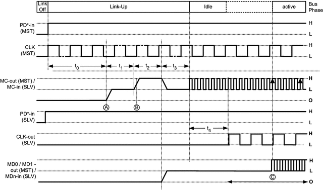
The Power_Down (PD*) input controls the power state of the MPL interface. When PD* is asserted, the MD1/0 and MC signals are powered down to save current.
The LM2502 implements the physical layer of the MPL Standard (MPL-0). The LM2502 is offered in NOPB (Lead-free) NFBGA and WQFN packages.


