ADS62P49 Series
Dual-Channel, 14-Bit, 250-MSPS Analog-to-Digital Converter (ADC)
Manufacturer: Texas Instruments
Catalog
Dual-Channel, 14-Bit, 250-MSPS Analog-to-Digital Converter (ADC)
Key Features
• Maximum Sample Rate: 250 MSPS14-Bit Resolution – ADS62P49/ADS62P4812-Bit Resolution – ADS62P29/ADS62P28Total Power: 1.25 W at 250 MSPSDouble Data Rate (DDR) LVDS and Parallel CMOS Output OptionsProgrammable Gain up to 6dB for SNR/SFDR Trade-OffDC Offset Correction90dB Cross-TalkSupports Input Clock Amplitude Down to 400 mVPPDifferentialInternal and External Reference Support64-QFN Package (9 mm × 9 mm)Maximum Sample Rate: 250 MSPS14-Bit Resolution – ADS62P49/ADS62P4812-Bit Resolution – ADS62P29/ADS62P28Total Power: 1.25 W at 250 MSPSDouble Data Rate (DDR) LVDS and Parallel CMOS Output OptionsProgrammable Gain up to 6dB for SNR/SFDR Trade-OffDC Offset Correction90dB Cross-TalkSupports Input Clock Amplitude Down to 400 mVPPDifferentialInternal and External Reference Support64-QFN Package (9 mm × 9 mm)
Description
AI
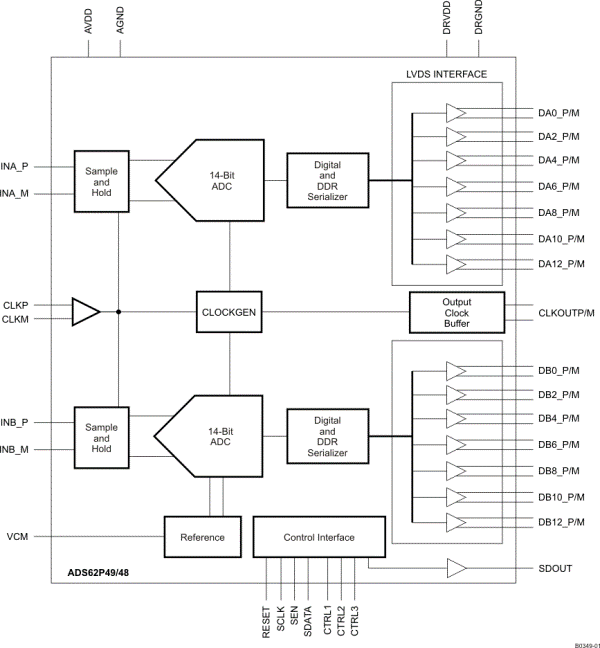
The ADS62Px9/x8 is a family of dual channel 14-bit and 12-bit A/D converters with sampling rates up to 250 MSPS. It combines high dynamic performance and low power consumption in a compact 64 QFN package. This makes it well-suited for multi-carrier, wide band-width communications applications.
The ADS62Px9/x8 has gain options that can be used to improve SFDR performance at lower full-scale input ranges. It includes a dc offset correction loop that can be used to cancel the ADC offset. Both DDR LVDS (Double Data Rate) and parallel CMOS digital output interfaces are available.
It includes internal references while the traditional reference pins and associated decoupling capacitors have been eliminated. Nevertheless, the device can also be driven with an external reference. The device is specified over the industrial temperature range (–40°C to 85°C).


