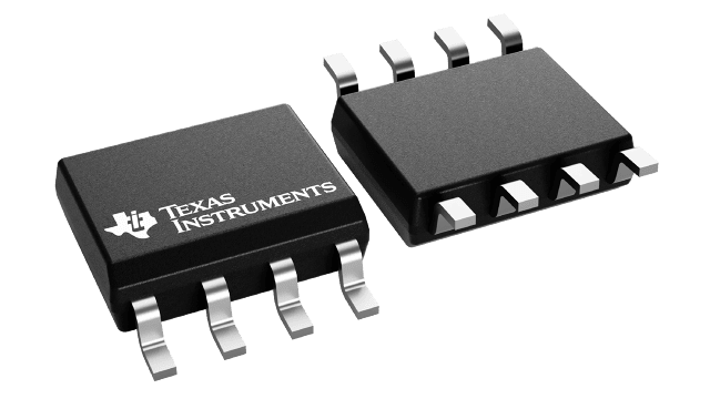
TLC1078 Series
Dual Micropower Precision Low-Voltage Operational Amplifier
Manufacturer: Texas Instruments
Catalog
Dual Micropower Precision Low-Voltage Operational Amplifier
Key Features
• Power Dissipation as Low as 10 uW Typ Per AmplifierOperates on a Single Silver-Oxide Watch Battery, VDD= 1.4 V MinVIO...450 uV/850 uV Max in DIP and Small-Outline Package (TLC1078/79)Input Offset Voltage Drift...0.1 uV/Month Typ, Including the First 30 DaysHigh-impedance LinCMOSTMInputsIIB= 0.6 pA TypHigh Open-Loop Gain...800000 TypOutput Drive Capability > 20 mASlew Rate...47 V/ms TypCommon-Mode Input Voltage Range Extends Below the Negative RailOutput Voltage Range Includes Negative RailOn-Chip ESD-Protection CircuitrySmall-Outline Package Option Also Available in Tape and ReelLinCMOS is a trademark of Texas Instruments Incorporated.Power Dissipation as Low as 10 uW Typ Per AmplifierOperates on a Single Silver-Oxide Watch Battery, VDD= 1.4 V MinVIO...450 uV/850 uV Max in DIP and Small-Outline Package (TLC1078/79)Input Offset Voltage Drift...0.1 uV/Month Typ, Including the First 30 DaysHigh-impedance LinCMOSTMInputsIIB= 0.6 pA TypHigh Open-Loop Gain...800000 TypOutput Drive Capability > 20 mASlew Rate...47 V/ms TypCommon-Mode Input Voltage Range Extends Below the Negative RailOutput Voltage Range Includes Negative RailOn-Chip ESD-Protection CircuitrySmall-Outline Package Option Also Available in Tape and ReelLinCMOS is a trademark of Texas Instruments Incorporated.
Description
AI
The TLC107x operational amplifiers offer ultra-low offset voltage, high gain, 110-kHz bandwidth, 47-V/ms slew rate, and just 150-uW power dissipation per amplifier.
With a supply voltage of 1.4 V, common-mode input to the negative rail, and output swing to the negative rail, the TLC107xC is an ideal solution for low-voltage battery-operated systems. The 20-mA output drive capability means that the TLC107x can easily drive small resistive and large capacitive loads when needed, while maintaining ultra-low standby power dissipation.
Since this device is functionally compatible as well as pin compatible with the TLC27L2/4 and TLC27L7/9, the TLC107x easily upgrades existing designs that can benefit from its improved performance.
The TLC107x incorporates internal ESD-protection circuits that will prevent functional failures at voltages up to 2000 V as tested under MIL-PRF-38535, Method 3015.2; however, care should be exercised when handling these devices as exposure to ESD may result in degradation of the device parametric performance. The TLC107x design also inhibits latch-up of the device inputs and outputs even with surge currents as large 100 mA.
The C-suffix devices are characterized for operation from 0°C to 70°C. The I-suffix devices are characterized for operation from -40°C to 85°C. The M-suffix devices are characterized for operation over the full military temperature range of -55°C to 125°C. The wide range of packaging options includes small-outline and chip-carrier versions for high-density system applications.


