SCAN921226H Series
High temperature 20 to 80-MHz 10-bit deserializer with IEEE 1149.1 test access
Manufacturer: Texas Instruments
Catalog
High temperature 20 to 80-MHz 10-bit deserializer with IEEE 1149.1 test access
Key Features
• High Temperature Operation to 125°CIEEE 1149.1 (JTAG) Compliant and At-Speed BIST Test ModeClock Recovery from PLL Lock to Random Data PatternsEnsured Transition Every Data Transfer CycleChipset (Tx + Rx) Power Consumption < 600 mW (Typ) @ 80 MHzSingle Differential Pair Eliminates Multi-Channel Skew800 Mbps Serial Bus LVDS Data Rate (at 80 MHz Clock)10-bit Parallel Interface for 1 Byte Data Plus 2 Control BitsSynchronization Mode and LOCK IndicatorProgrammable Edge Trigger on ClockHigh Impedance on Receiver Inputs When Power is OffBus LVDS Serial Output Rated for 27Ω LoadSmall 49-Lead NFBGA PackageAll trademarks are the property of their respective owners.High Temperature Operation to 125°CIEEE 1149.1 (JTAG) Compliant and At-Speed BIST Test ModeClock Recovery from PLL Lock to Random Data PatternsEnsured Transition Every Data Transfer CycleChipset (Tx + Rx) Power Consumption < 600 mW (Typ) @ 80 MHzSingle Differential Pair Eliminates Multi-Channel Skew800 Mbps Serial Bus LVDS Data Rate (at 80 MHz Clock)10-bit Parallel Interface for 1 Byte Data Plus 2 Control BitsSynchronization Mode and LOCK IndicatorProgrammable Edge Trigger on ClockHigh Impedance on Receiver Inputs When Power is OffBus LVDS Serial Output Rated for 27Ω LoadSmall 49-Lead NFBGA PackageAll trademarks are the property of their respective owners.
Description
AI
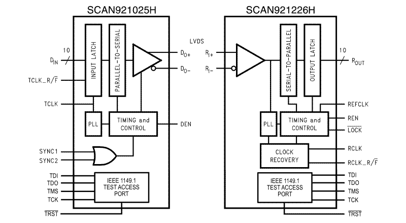
The SCAN921025H transforms a 10-bit wide parallel LVCMOS/LVTTL data bus into a single high speed Bus LVDS serial data stream with embedded clock. The SCAN921226H receives the Bus LVDS serial data stream and transforms it back into a 10-bit wide parallel data bus and recovers parallel clock.
Both devices are compliant with IEEE 1149.1 Standard for Boundary Scan Test. IEEE 1149.1 features provide the design or test engineer access via a standard Test Access Port (TAP) to the backplane or cable interconnects and the ability to verify differential signal integrity. The pair of devices also features an at-speed BIST mode which allows the interconnects between the Serializer and Deserializer to be verified at-speed.
The SCAN921025H transmits data over backplanes or cable. The single differential pair data path makes PCB design easier. In addition, the reduced cable, PCB trace count, and connector size tremendously reduce cost. Since one output transmits clock and data bits serially, it eliminates clock-to-data and data-to-data skew. The powerdown pin saves power by reducing supply current when not using either device. Upon power up of the Serializer, you can choose to activate synchronization mode or allow the Deserializer to use the synchronization-to-random-data feature. By using the synchronization mode, the Deserializer will establish lock to a signal within specified lock times. In addition, the embedded clock ensures a transition on the bus every 12-bit cycle. This eliminates transmission errors due to charged cable conditions. Furthermore, you may put the SCAN921025H output pins into tri-state to achieve a high impedance state. The PLL can lock to frequencies between 20 MHz and 80 MHz.


