LM51581-Q1 Series
1.5-A, 85-V, 2.2-MHz wide VIN boost, flyback, & SEPIC converter with dual random spread spectrum
Manufacturer: Texas Instruments
Catalog
1.5-A, 85-V, 2.2-MHz wide VIN boost, flyback, & SEPIC converter with dual random spread spectrum
Key Features
• AEC-Q100 qualified for automotive applicationsTemperature grade 1: –40°C to +125°C TAFunctional Safety-CapableDocumentation available to aid functional safety system designSuited for wide operating range for car battery applications3.2-V to 60-V input operating range (65-V abs max)83-V maximum output (85-V abs max)Minimum boost supply voltage of 1.5 V when BIAS ≥ 3.2 VInput transient protection up to 65 VMinimized battery drainLow shutdown current (IQ≤ 2.6 µA)Low operating current (IQ≤ 670 µA)Small solution size and low costMaximum switching frequency up to 2.2 MHz16-pin QFN package (3 mm × 3 mm) with wettable flanksIntegrated error amplifier allows primary-side regulation without optocoupler (flyback)Minimized undershoot during crankingAccurate current limit (see theDevice Comparison Table)EMI mitigationSelectable dual random spread spectrumLead-less packageHigher efficiency with low-power dissipation133-mΩ RDSONswitchFast switching, small switching lossAvoid AM band interference and crosstalkOptional clock synchronizationDynamically programmable wide switching frequency from 100 kHz to 2.2 MHzIntegrated protection featuresConstant current limiting over input voltageSelectable hiccup mode overload protectionProgrammable line UVLOOVP protectionThermal shutdownAccurate ±1% accuracy feedback referenceAdjustable soft startPGOOD indicatorCreate a custom design using the LM5158x -Q1 with theWEBENCH Power DesignerAEC-Q100 qualified for automotive applicationsTemperature grade 1: –40°C to +125°C TAFunctional Safety-CapableDocumentation available to aid functional safety system designSuited for wide operating range for car battery applications3.2-V to 60-V input operating range (65-V abs max)83-V maximum output (85-V abs max)Minimum boost supply voltage of 1.5 V when BIAS ≥ 3.2 VInput transient protection up to 65 VMinimized battery drainLow shutdown current (IQ≤ 2.6 µA)Low operating current (IQ≤ 670 µA)Small solution size and low costMaximum switching frequency up to 2.2 MHz16-pin QFN package (3 mm × 3 mm) with wettable flanksIntegrated error amplifier allows primary-side regulation without optocoupler (flyback)Minimized undershoot during crankingAccurate current limit (see theDevice Comparison Table)EMI mitigationSelectable dual random spread spectrumLead-less packageHigher efficiency with low-power dissipation133-mΩ RDSONswitchFast switching, small switching lossAvoid AM band interference and crosstalkOptional clock synchronizationDynamically programmable wide switching frequency from 100 kHz to 2.2 MHzIntegrated protection featuresConstant current limiting over input voltageSelectable hiccup mode overload protectionProgrammable line UVLOOVP protectionThermal shutdownAccurate ±1% accuracy feedback referenceAdjustable soft startPGOOD indicatorCreate a custom design using the LM5158x -Q1 with theWEBENCH Power Designer
Description
AI
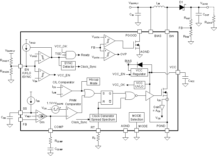
The LM5158x -Q1 device is a wide input range, non-synchronous boost converter with an integrated 85-V, 3.26-A (LM5158 -Q1) or 85-V, 1.63-A (LM51581 -Q1) power switch.
The device can be used in boost, SEPIC, and flyback topologies. It can start up from a single-cell battery with a minimum of 3.2 V. It can operate with the input supply voltage as low as 1.5 V if the BIAS pin is greater than 3.2 V.
The BIAS pin operates up to 60 V (65-V absolute maximum) for automotive load dump. The switching frequency is dynamically programmable from 100 kHz to 2.2 MHz with an external resistor. Switching at 2.2 MHz minimizes AM band interference and allows for a small solution size and fast transient response. The device provides a selectable Dual Random Spread Spectrum to help reduce the EMI over a wide frequency range.
The device features an accurate peak current limit over the input voltage, which avoids overdesigning the power inductor. Low operating current and pulse-skipping operation improve efficiency at light loads.
The device has built-in protection features such as overvoltage protection, line UVLO, thermal shutdown, and selectable hiccup mode overload protection. Additional features include low shutdown IQ, programmable soft start, precision reference, a power-good indicator, and external clock synchronization.


