Catalog
8-bit open-collector driver with Latch
Key Features
• LBC3S (Lin BiCMOS) ProcessHigh Voltage Output (VOUT= 24 V)Output Current (IOLMaximum = 40 mA)Latch-Up Performance Exceeds 250 mA PerJEDEC Standard JESD-17ESD Protection Exceeds JESD 222000-V Human Body Model (A114-A)200-V Machine Model (A115-A)1000-V Charged Device Model (C101)LBC3S (Lin BiCMOS) ProcessHigh Voltage Output (VOUT= 24 V)Output Current (IOLMaximum = 40 mA)Latch-Up Performance Exceeds 250 mA PerJEDEC Standard JESD-17ESD Protection Exceeds JESD 222000-V Human Body Model (A114-A)200-V Machine Model (A115-A)1000-V Charged Device Model (C101)
Description
AI
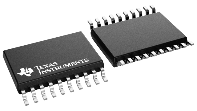
The TLC59212 device is an 8-bit open-collector driver with latch designed for 5-V VCCoperation.
These circuits are positive-edge-triggered D-type flip-flops with a direct clear (CLR) input. Information at the data (D) input meeting the setup time requirements is transferred to theYoutput on the positive-going edge of the clock (CLK) pulse. Clock triggering occurs at a particular voltage level and is not directly related to the transition time of the positive-going pulse. When CLK is at either the high or low level, the D-input has no effect at the output.
The TLC59212 is characterized for operation from –40°C to 85°C.


