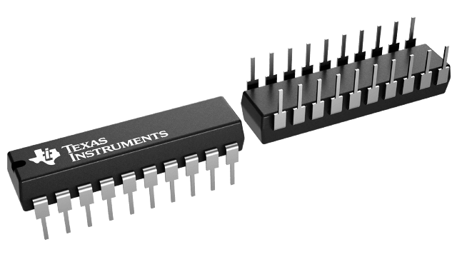
CY74FCT245T Series
BiCMOS FCT Interface Logic Octal Non-Inverting Bus Transceivers with 3-State Outputs
Manufacturer: Texas Instruments
Catalog
BiCMOS FCT Interface Logic Octal Non-Inverting Bus Transceivers with 3-State Outputs
Key Features
• Function, Pinout, and Drive Compatible With FCT and F LogicReduced VOH(Typically = 3.3 V) Versions of Equivalent FCT FunctionsEdge-Rate Control Circuitry for Significantly Improved Noise CharacteristicsIoffSupports Partial-Power-Down Mode OperationESD Protection Exceeds JESD 222000-V Human-Body Model (A114-A)200-V Machine Model (A115-A)1000-V Charged-Device Model (C101)Matched Rise and Fall TimesFully Compatible With TTL Input and Output Logic LevelsCY54FCT245T48-mA Output Sink Current12-mA Output Source CurrentCY74FCT245T64-mA Output Sink Current32-mA Output Source Current3-State OutputsFunction, Pinout, and Drive Compatible With FCT and F LogicReduced VOH(Typically = 3.3 V) Versions of Equivalent FCT FunctionsEdge-Rate Control Circuitry for Significantly Improved Noise CharacteristicsIoffSupports Partial-Power-Down Mode OperationESD Protection Exceeds JESD 222000-V Human-Body Model (A114-A)200-V Machine Model (A115-A)1000-V Charged-Device Model (C101)Matched Rise and Fall TimesFully Compatible With TTL Input and Output Logic LevelsCY54FCT245T48-mA Output Sink Current12-mA Output Source CurrentCY74FCT245T64-mA Output Sink Current32-mA Output Source Current3-State Outputs
Description
AI
The CD74FCT245 is an octal bus transceiver with 3-state outputs using a small-geometry BiCMOS technology. The output stages are a combination of bipolar and CMOS transistors that limit the output high level to two diode drops below VCC. This resultant lowering of output swing (0 V to 3.7 V) reduces the power-bus ringing [a source of electromagnetic interference (EMI)] and minimizes VCCbounce and ground bounce and their effects during simultaneous output switching. The output configuration also enhances switching speed and is capable of sinking 64 mA.
The CD74FCT245 allows data transmission from the A bus to the B bus or from the B bus to the A bus, depending upon the logic level at the direction-control (DIR) input. The output-enable (OE\) input can be used to disable the device so that the buses are effectively isolated.
To ensure the high-impedance state during power up or power down, OE\ should be tied to VCCthrough a pullup resistor; the minimum value of the resistor is determined by the current-sinking capability of the driver.
The CD74FCT245 is characterized for operation from 0°C to 70°C.


