Catalog
Automotive single 1.65-V to 5.5-V inverter
Key Features
• Qualified for Automotive ApplicationsAEC-Q100 Qualified with the Following ResultsDevice Temperature Grade 1:–40°C to 125°C Ambient Operating Temperature RangeDevice HBM ESD Classification Level H2Device CDM ESG Classification Level C4BESD Protection Exceeds 2000 V Per MIL-STD-883, Method 3015;Exceeds 200 V Using Machine Model (C = 200 pF, R = 0)Supports 5-V VCCOperationInputs Accept Voltages to 5.5 VMax tpdof 3.3 ns at 3.3 VLow Power Consumption, 10-µA Max ICC±24-mA Output Drive at 3.3 VIoffSupports Partial-Power-Down Mode OperationLatch-Up Performance Exceeds 100 mA Per JESD 78, Class IIQualified for Automotive ApplicationsAEC-Q100 Qualified with the Following ResultsDevice Temperature Grade 1:–40°C to 125°C Ambient Operating Temperature RangeDevice HBM ESD Classification Level H2Device CDM ESG Classification Level C4BESD Protection Exceeds 2000 V Per MIL-STD-883, Method 3015;Exceeds 200 V Using Machine Model (C = 200 pF, R = 0)Supports 5-V VCCOperationInputs Accept Voltages to 5.5 VMax tpdof 3.3 ns at 3.3 VLow Power Consumption, 10-µA Max ICC±24-mA Output Drive at 3.3 VIoffSupports Partial-Power-Down Mode OperationLatch-Up Performance Exceeds 100 mA Per JESD 78, Class II
Description
AI
This single inverter gate is designed for1.65-V to 5.5-V VCCoperation.
The SN74LVC1G04 device performs the Boolean function Y =A.
The CMOS device has high output drive while maintaining low static power dissipation over a broad VCCoperating range.
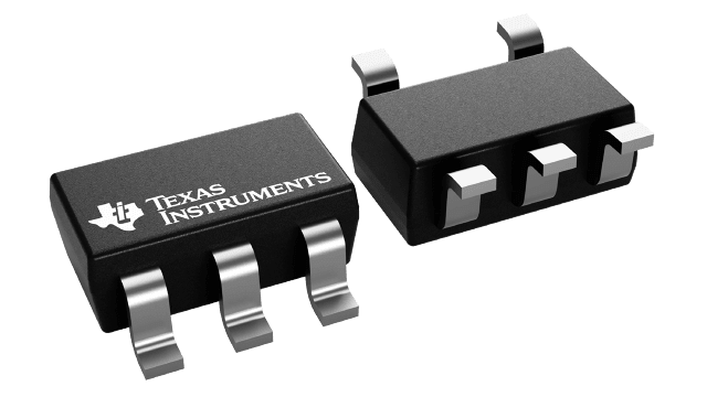
The SN74LVC1G04 device is available in a variety of packages, including the ultra-small DPW package with a body size of 0.8 mm × 0.8 mm.


