ADC08B3000 Series
8-Bit, 3.0-GSPS Analog-to-Digital Converter (ADC) with 4K Buffer
Manufacturer: Texas Instruments
Catalog
8-Bit, 3.0-GSPS Analog-to-Digital Converter (ADC) with 4K Buffer
| Part | Supplier Device Package | Operating Temperature [Max] | Operating Temperature [Min] | Configuration | Number of Inputs | Voltage - Supply, Analog [Min] | Voltage - Supply, Analog [Max] | Voltage - Supply, Digital [Max] | Voltage - Supply, Digital [Min] | Reference Type | Input Type | Sampling Rate (Per Second) | Architecture | Ratio - S/H:ADC | Number of A/D Converters | Mounting Type | Data Interface | Number of Bits |
|---|---|---|---|---|---|---|---|---|---|---|---|---|---|---|---|---|---|---|
Texas Instruments | 128-HLQFP (20x20) | 85 °C | -40 °C | S/H-ADC | 1 | 1.8 V | 2 V | 2 V | 1.8 V | Internal | Differential | 3 G | Folding Interpolating | 2:2 | 1 | Surface Mount | Parallel SPI | 8 |
Key Features
• Single +1.9V ±0.1V OperationChoice of SDR or DDR Output ClockingInternal selectable 4K Data BufferSerial Interface for Extended ControlAdjustment of Input Full-Scale Range, Offset and Clock PhaseDuty Cycle Corrected Sample ClockTest Pattern Output CapabilityKey SpecificationsResolution: 8 BitsMax Conversion Rate: 3 Gsps (min)Code Error Rate: 10-18(typ)ENOB @ 748 MHz Input: 7.1 Bits (typ)SNR @ 748 MHz: 44.9 dB (typ)Full Power Bandwidth: 3 GHz (typ)Power ConsumptionFull Power Capure: 1.6 W (typ)Power Down Mode: 25 mW (typ)All trademarks are the property of their respective owners.Single +1.9V ±0.1V OperationChoice of SDR or DDR Output ClockingInternal selectable 4K Data BufferSerial Interface for Extended ControlAdjustment of Input Full-Scale Range, Offset and Clock PhaseDuty Cycle Corrected Sample ClockTest Pattern Output CapabilityKey SpecificationsResolution: 8 BitsMax Conversion Rate: 3 Gsps (min)Code Error Rate: 10-18(typ)ENOB @ 748 MHz Input: 7.1 Bits (typ)SNR @ 748 MHz: 44.9 dB (typ)Full Power Bandwidth: 3 GHz (typ)Power ConsumptionFull Power Capure: 1.6 W (typ)Power Down Mode: 25 mW (typ)All trademarks are the property of their respective owners.
Description
AI
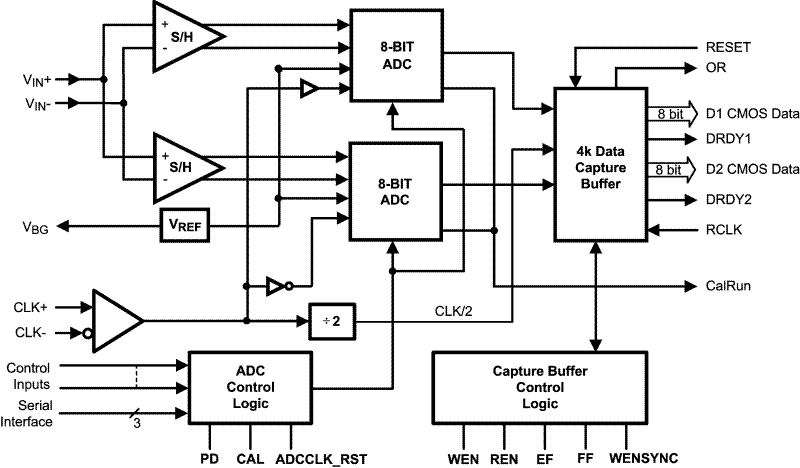
The ADC08B3000 is a single, low power, high performance CMOS analog-to-digital converter that digitizes signals to 8 bits resolution at sample rates up to 3.4 Gigasamples Per Second, (Gsps). Consuming a typical 1.6 Watts at 3 Gsps from a single 1.9 Volt supply, this device is ensured to have no missing codes over the full operating temperature range. The unique folding and interpolating architecture, the fully differential comparator design, the innovative design of the internal sample-and-hold amplifier and the calibration scheme enable an excellent response of all dynamic parameters up to Nyquist, producing a high 7.1 Effective Number Of Bits, (ENOB), with a 748 MHz input signal and a 3 GHz sample rate while providing a 10-18Code Error Rate. A sample rate of 3 Gsps is achieved by interleaving two ADCs, each operating at 1.5 Gsps. Output formatting is offset binary. The device contains a 4K Capture Buffer with output on two 8-bit Low Voltage CMOS (LVCMOS) output buses at rates up to 200MHz.
The converter typically consumes less than 25 mW in the Power Down Mode and is available in a 128-lead, thermally enhanced exposed pad HLQFP and operates over the Industrial (-40°C ≤ TA≤ +85°C) temperature range.


