DRV8301-Q1 Series
65-V max 3-phase gate driver with buck regulator, current shunt amplifiers & SPI
Manufacturer: Texas Instruments
Catalog
65-V max 3-phase gate driver with buck regulator, current shunt amplifiers & SPI
Key Features
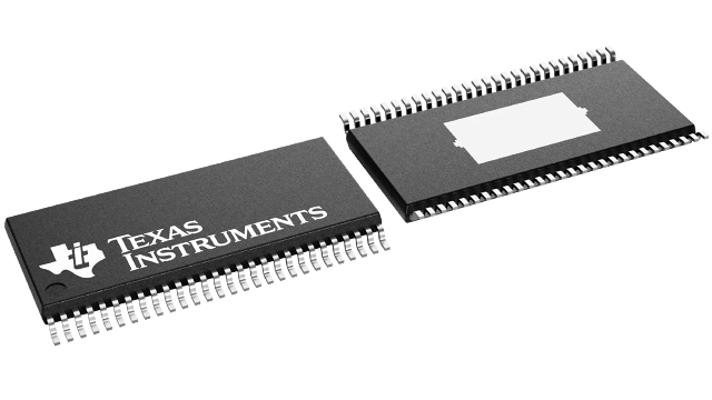
• Qualified for Automotive ApplicationsAEC-Q100 Tested With the Following Results:Device Temperature Grade 1: –40°C to 125°CAmbient Operating Temperature RangeDevice HBM ESD Classification Level 2Device CDM ESD Classification Level C4AOperating Supply Voltage 6 to 60 V2.3-A Sink and 1.7-A Source Gate Drive CurrentCapabilityIntegrated Dual Shunt Current Amplifiers WithAdjustable Gain and OffsetIntegrated Buck Converter to Support up to 1.5-AExternal LoadIndependent Control of 3 or 6 PWM InputsBootstrap Gate Driver With 100% Duty CycleSupportProgrammable Dead Time to Protect ExternalFETs from Shoot-ThroughSlew Rate Control for EMI ReductionProgrammable Overcurrent Protection of ExternalMOSFETsSupport Both 3.3-V and 5-V Digital InterfaceSPI InterfaceThermally Enhanced 56-Pin HTSSOP Pad-DownDCA PackageQualified for Automotive ApplicationsAEC-Q100 Tested With the Following Results:Device Temperature Grade 1: –40°C to 125°CAmbient Operating Temperature RangeDevice HBM ESD Classification Level 2Device CDM ESD Classification Level C4AOperating Supply Voltage 6 to 60 V2.3-A Sink and 1.7-A Source Gate Drive CurrentCapabilityIntegrated Dual Shunt Current Amplifiers WithAdjustable Gain and OffsetIntegrated Buck Converter to Support up to 1.5-AExternal LoadIndependent Control of 3 or 6 PWM InputsBootstrap Gate Driver With 100% Duty CycleSupportProgrammable Dead Time to Protect ExternalFETs from Shoot-ThroughSlew Rate Control for EMI ReductionProgrammable Overcurrent Protection of ExternalMOSFETsSupport Both 3.3-V and 5-V Digital InterfaceSPI InterfaceThermally Enhanced 56-Pin HTSSOP Pad-DownDCA Package
Description
AI
The DRV8301-Q1 device is an automotive gate driver IC for three phase motor drive applications. The device provides three half bridge drivers, each capable of driving two N-type MOSFETs, one for the high-side and one for the low side. The device supports up to 2.3-A sink and 1.7-A source peak current capability and only needs a single power supply with a wide range from 6 to 60 V. The DRV8301-Q1 device uses bootstrap gate drivers with trickle charge circuitry to support 100% duty cycle. The gate driver uses automatic hand shaking when high-side FET or low-side FET is switching to prevent current shoot through. VDSof FETs is sensed to protect external power stage during overcurrent conditions.
The DRV8301-Q1 device includes two current shunt amplifiers for accurate current measurement. The current amplifiers support bi-directional current sensing and provide an adjustable output offset of up to 3 V.
The DRV8301-Q1 device also has an integrated switching mode buck converter with adjustable output and switching frequency to support MCU or additional system power needs. The buck is capable to drive up to 1.5-A load.
The SPI interface provides detailed fault reporting and flexible parameter settings such as gain options for current shunt amplifier, slew rate control of gate driver, and other settings.


