TPS22968-Q1 Series
2-ch, 5.5-V, 4-A, 27-mΩ, automotive load switch with adj. rise time and output discharge
Manufacturer: Texas Instruments
Catalog
2-ch, 5.5-V, 4-A, 27-mΩ, automotive load switch with adj. rise time and output discharge
Key Features
• Integrated Dual Channel Load SwitchInput Voltage Range: 0.8 V to 5.5 VVBIAS Voltage Range: 2.5 V to 5.5 VIdeal for 1S Battery ConfigurationUltra-Low RONResistanceRON= 27 mΩ at VIN= 5 V (VBIAS= 5 V)RON= 25 mΩ at VIN= 3.3 V (VBIAS= 5 V)RON= 25 mΩ at VIN= 1.8 V (VBIAS= 5 V)4-A Maximum Continuous Switch Current per ChannelLow Quiescent Current55 µA at VBIAS= 5 V (Both Channels)55 µA at VBIAS= 5 V (Single Channel)Low Control Input Threshold Enables Use of1.2-,1.8-, 2.5-, 3.3-V LogicConfigurable Rise Time(1)Quick Output Discharge (QOD)(2)(Optional)SON 14-Pin Package with Thermal PadESD Performance Tested per JEDEC Standard2-kV HBM and 1-kV CDMLatch-Up Performance Exceeds 100 mA per JESD 78, Class IIGPIO Enable – Active HighTPS22968N: Product Preview Only(1)(2)(1)See theApplication Informationsection for CT value vs. rise time(2)This feature discharges the output of the switch to GND through a 270-Ω resistor, preventing the output from floating.Integrated Dual Channel Load SwitchInput Voltage Range: 0.8 V to 5.5 VVBIAS Voltage Range: 2.5 V to 5.5 VIdeal for 1S Battery ConfigurationUltra-Low RONResistanceRON= 27 mΩ at VIN= 5 V (VBIAS= 5 V)RON= 25 mΩ at VIN= 3.3 V (VBIAS= 5 V)RON= 25 mΩ at VIN= 1.8 V (VBIAS= 5 V)4-A Maximum Continuous Switch Current per ChannelLow Quiescent Current55 µA at VBIAS= 5 V (Both Channels)55 µA at VBIAS= 5 V (Single Channel)Low Control Input Threshold Enables Use of1.2-,1.8-, 2.5-, 3.3-V LogicConfigurable Rise Time(1)Quick Output Discharge (QOD)(2)(Optional)SON 14-Pin Package with Thermal PadESD Performance Tested per JEDEC Standard2-kV HBM and 1-kV CDMLatch-Up Performance Exceeds 100 mA per JESD 78, Class IIGPIO Enable – Active HighTPS22968N: Product Preview Only(1)(2)(1)See theApplication Informationsection for CT value vs. rise time(2)This feature discharges the output of the switch to GND through a 270-Ω resistor, preventing the output from floating.
Description
AI
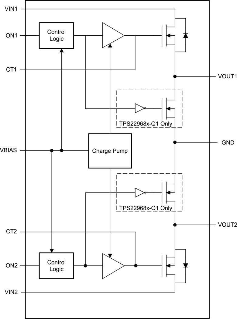
The TPS22968x-Q1 is a small, dual-channel load switch with configurable rise time. The device contains two N-channel MOSFETs that can operate over an input voltage range of 0.8 V to 5.5 V and can support a maximum continuous current of 4-A per channel. Each switch is independently controlled by an on/off input (ON1 and ON2), which is capable of interfacing directly with low-voltage control signals. The TPS22968-Q1 includes a 270 Ω on-chip resistor for quick output discharge when the switch is turned off.
The TPS22968x-Q1 is available in a small, space-saving package (DMG) with wettable flanks and an integrated thermal pad. The wettable flanks allow for visual solder inspection. The device is characterized for operation over the free-air temperature range of –40 to +125°C.


