Catalog
5.5-V, 2-A, 39-mΩ load switch with output discharge
Key Features
• Integrated Single Channel Load SwitchInput Voltage Range: 1.05 V to 5.5 VLow On-Resistance (RON)RON= 37 mΩ (Typical) at VIN= 5 VRON= 38 mΩ (Typical) at VIN= 3.3 VRON= 43 mΩ (Typical) at VIN= 1.8 V2-A Maximum Continuous Switch CurrentLow Quiescent Current7.7 µA (Typical) at VIN= 3.3 VLow Control Input Threshold Enables Use of 1 V or Higher GPIOControlled Slew RatetR(TPS22914B/15B) = 64 µs at VIN= 3.3 VtR(TPS22914C/15C) = 913 µs at VIN= 3.3 VQuick Output Discharge (TPS22915 only)Ultra-Small Wafer-Chip-Scale Package0.78 mm × 0.78 mm, 0.4-mm Pitch, 0.5-mm Height (YFP)ESD Performance Tested per JESD 222-kV HBM and 1-kV CDMIntegrated Single Channel Load SwitchInput Voltage Range: 1.05 V to 5.5 VLow On-Resistance (RON)RON= 37 mΩ (Typical) at VIN= 5 VRON= 38 mΩ (Typical) at VIN= 3.3 VRON= 43 mΩ (Typical) at VIN= 1.8 V2-A Maximum Continuous Switch CurrentLow Quiescent Current7.7 µA (Typical) at VIN= 3.3 VLow Control Input Threshold Enables Use of 1 V or Higher GPIOControlled Slew RatetR(TPS22914B/15B) = 64 µs at VIN= 3.3 VtR(TPS22914C/15C) = 913 µs at VIN= 3.3 VQuick Output Discharge (TPS22915 only)Ultra-Small Wafer-Chip-Scale Package0.78 mm × 0.78 mm, 0.4-mm Pitch, 0.5-mm Height (YFP)ESD Performance Tested per JESD 222-kV HBM and 1-kV CDM
Description
AI
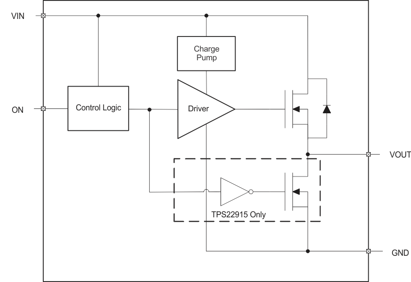
The TPS22914/15 is a small, low RON, single channel load switch with controlled slew rate. The device contains an N-channel MOSFET that can operate over an input voltage range of 1.05 V to 5.5 V and can support a maximum continuous current of 2 A. The switch is controlled by an on and off input, which is capable of interfacing directly with low-voltage control signals.
The small size and low RONmakes the device ideal for being used in space constrained, battery powered applications. The wide input voltage range of the switch makes it a versatile solution for many different voltage rails. The controlled rise time of the device greatly reduces inrush current caused by large bulk load capacitances, thereby reducing or eliminating power supply droop. The TPS22915 further reduces the total solution size by integrating a 143-Ω pull-down resistor for quick output discharge (QOD) when the switch is turned off.
The TPS22914/15 is available in a small, space-saving 0.78 mm x 0.78 mm, 0.4-mm pitch, 0.5-mm height 4-pin Wafer-Chip-Scale (WCSP) package (YFP). The device is characterized for operation over the free-air temperature range of –40°C to +105°C.


