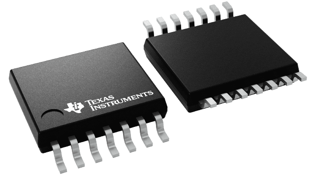
SN74CB3T3125 Series
3.3-V, 1:1 (SPST), 4-channel FET bus switch with level shifter
Manufacturer: Texas Instruments
Catalog
3.3-V, 1:1 (SPST), 4-channel FET bus switch with level shifter
Key Features
• Output Voltage Translation Tracks VCCSupports Mixed-Mode Signal Operation On All Data I/O Ports5-V Input Down to 3.3-V Output-Level Shift With 3.3-V VCC5-V/3.3-V Input Down to 2.5-V Output-Level Shift With 2.5-V VCC5-V-Tolerant I/Os With Device Powered Up or Powered DownBidirectional Data Flow, With Near-Zero Propagation DelayLow ON-State Resistance (ron) Characteristics(ron= 5 Ω Typical)Low Input/Output Capacitance Minimizes Loading(Cio(OFF)= 4.5 pF Typical)Data and Control Inputs Provide Undershoot Clamp DiodesLow Power Consumption (ICC= 20 µA Max)VCCOperating Range From 2.3 V to 3.6 VData I/Os Support 0- to 5-V Signaling Levels (0.8 V, 1.2 V, 1.5 V, 1.8 V, 2.5 V, 3.3 V, 5 V)Control Inputs Can Be Driven by TTL or 5-V/3.3-V CMOS OutputsIoffSupports Partial-Power-Down Mode OperationLatch-Up Performance Exceeds 250 mA Per JESD 17ESD Performance Tested Per JESD 222000-V Human-Body Model(A114-B, Class II)1000-V Charged-Device Model (C101)Output Voltage Translation Tracks VCCSupports Mixed-Mode Signal Operation On All Data I/O Ports5-V Input Down to 3.3-V Output-Level Shift With 3.3-V VCC5-V/3.3-V Input Down to 2.5-V Output-Level Shift With 2.5-V VCC5-V-Tolerant I/Os With Device Powered Up or Powered DownBidirectional Data Flow, With Near-Zero Propagation DelayLow ON-State Resistance (ron) Characteristics(ron= 5 Ω Typical)Low Input/Output Capacitance Minimizes Loading(Cio(OFF)= 4.5 pF Typical)Data and Control Inputs Provide Undershoot Clamp DiodesLow Power Consumption (ICC= 20 µA Max)VCCOperating Range From 2.3 V to 3.6 VData I/Os Support 0- to 5-V Signaling Levels (0.8 V, 1.2 V, 1.5 V, 1.8 V, 2.5 V, 3.3 V, 5 V)Control Inputs Can Be Driven by TTL or 5-V/3.3-V CMOS OutputsIoffSupports Partial-Power-Down Mode OperationLatch-Up Performance Exceeds 250 mA Per JESD 17ESD Performance Tested Per JESD 222000-V Human-Body Model(A114-B, Class II)1000-V Charged-Device Model (C101)
Description
AI
The SN74CB3T3125 is a high-speed TTL-compatible FET bus switch with low ON-state resistance (ron), allowing for minimal propagation delay. The device fully supports mixed-mode signal operation on all data I/O ports by providing voltage translation that tracks VCC. The SN74CB3T3125 supports systems using 5-V TTL, 3.3-V LVTTL, and 2.5-V CMOS switching standards, as well as user-defined switching levels (seeTypical DC Voltage-Translation Characteristics).
The SN74CB3T3125 is organized as four 1-bit bus switches with separate output-enable (1OE, 2OE, 3OE, 4OE) inputs. It can be used as four 1-bit bus switches or as one 4-bit bus switch. WhenOEis low, the associated 1-bit bus switch is ON, and the A port is connected to the B port, allowing bidirectional data flow between ports. WhenOEis high, the associated 1-bit bus switch is OFF, and the high-impedance state exists between the A and B ports.
This device is fully specified for partial-power-down applications using Ioff. The Iofffeature ensures that damaging current will not backflow through the device when it is powered down. The device has isolation during power off.
To ensure the high-impedance state during power up or power down,OEshould be tied to VCCthrough a pullup resistor; the minimum value of the resistor is determined by the current-sinking capability of the driver.


